Thick copper PCBs represent a specialized category of printed circuit boards designed to handle substantial power requirements and thermal challenges. Unlike standard PCBs that typically feature 1oz to 2oz copper weights, thick copper boards incorporate copper layers exceeding 3oz, sometimes reaching as high as 20oz in specialized applications. This enhanced copper presence fundamentally transforms the electrical, thermal, and mechanical characteristics of the board, enabling performance capabilities unattainable with conventional PCB structures. The growing demand for robust power management solutions across automotive, renewable energy, and industrial sectors has catapulted thick copper PCB technology into a critical component of modern electronic design.
The distinction between standard and thick copper PCBs becomes particularly important when dealing with applications requiring high current capacity, superior thermal dissipation, or enhanced mechanical durability. The additional copper mass significantly reduces electrical resistance, improves heat distribution, and strengthens structural integrity—all critical factors in high-reliability electronic systems. Understanding the unique properties and manufacturing challenges of thick copper technology provides electronic engineers with powerful design options for addressing increasingly demanding power requirements.
Fundamentals of thick copper PCBs and their composition
Thick copper PCBs differ fundamentally from standard PCBs in both material composition and manufacturing processes. These specialized boards must balance the advantages of increased copper weight against the challenges of maintaining precise circuit geometries and ensuring proper adhesion between layers. The defining characteristic—copper thickness—transforms not just the electrical properties but also dictates specific requirements for substrate materials, fabrication techniques, and quality control measures.
Defining thick copper PCBs: classifications above 3oz copper weight
The industry generally classifies PCBs with copper weights at or exceeding 3oz (105μm) as thick copper boards. This classification creates an important distinction from standard PCBs that typically feature 1oz (35μm) or 2oz (70μm) copper weights. The copper weight measurement refers to the amount of copper covering one square foot of the PCB laminate—a direct indicator of thickness. For perspective, a 3oz copper layer measures approximately 105 micrometers thick, while heavier 10oz copper reaches 350 micrometers—nearly ten times thicker than standard 1oz copper layers.
According to icape-group.com, the classification system can be further refined into subcategories: heavy copper (3oz to 10oz) and extreme copper (above 10oz to 20oz). Each increment in copper weight introduces specific manufacturing challenges and design considerations, particularly regarding trace width, spacing requirements, and minimum feature sizes. Designers must carefully balance the benefits of increased current capacity against the limitations imposed on circuit density and overall board dimensions.
Core materials compatible with heavy copper deposition
Not all substrate materials can adequately support thick copper layers. The extreme temperatures and chemical processes involved in heavy copper deposition require substrates with exceptional thermal stability and mechanical strength. FR-4 remains the most common substrate for thick copper applications up to approximately 6oz, offering a reasonable balance between cost and performance. For applications exceeding 6oz copper or requiring superior thermal performance, specialized substrates become necessary.
High-Tg FR-4 variants (with glass transition temperatures above 170°C) provide enhanced thermal stability for thick copper applications, reducing the risk of delamination during manufacturing and operation. Polyimide substrates offer even greater thermal resistance and dimensional stability, making them suitable for extreme copper applications in high-temperature environments. For the most demanding thermal applications, metal core substrates—typically aluminum or copper core—provide direct thermal pathways that complement the heat-spreading capabilities of thick copper layers.
The selection of core material for thick copper PCBs represents one of the most critical design decisions, directly impacting manufacturing feasibility, thermal performance, and long-term reliability in harsh operating environments.
Copper plating techniques for High-Current applications
Achieving uniform copper deposition at thicknesses exceeding 3oz requires specialized electroplating processes that differ significantly from standard PCB fabrication. While thin copper PCBs can be produced using subtractive etching from copper-clad laminates, thick copper boards typically require additive or semi-additive processes. Pattern plating techniques become essential, where initial thin copper layers are selectively built up through multiple electroplating cycles.
For copper weights exceeding 6oz, manufacturers often employ panel plating followed by precise etching—a challenging process requiring tight control over chemical concentrations, current densities, and plating times. The pulse plating method has emerged as a powerful technique for achieving extremely uniform copper deposition even at high thicknesses. This approach alternates between plating and relaxation periods, allowing copper ions to distribute more evenly across the board surface, reducing the risk of nodules or voids that could compromise reliability.
Manufacturing tolerances and IPC-6012 standards for thick copper boards
The IPC-6012 standard establishes specific quality requirements for rigid printed boards, with special provisions for thick copper implementations. These standards define acceptable tolerances for conductor width, spacing, thickness variation, and plating uniformity. As copper thickness increases, maintaining tight manufacturing tolerances becomes exponentially more challenging, requiring specialized equipment and rigorous process controls.
For 3oz copper, the minimum recommended trace width typically starts at 10-12 mils, increasing proportionally with copper weight. At 10oz copper, minimum trace widths may exceed 30 mils, significantly impacting circuit density. Similarly, minimum spacing requirements increase from approximately 10 mils for 3oz copper to 25-30 mils for 10oz implementations. These expanded geometries ensure manufacturing reliability but present substantial design constraints that must be addressed early in the development process.
Thermal management properties of thick copper PCBs
The thermal management capabilities of thick copper PCBs represent one of their most valuable attributes for high-power applications. The substantially increased copper mass provides excellent thermal conductivity pathways that can efficiently distribute heat across the board surface. This inherent thermal spreading effect can dramatically reduce hotspot temperatures, extending component lifespans and improving system reliability under heavy loads.
Heat dissipation mechanisms in 4oz-10oz copper traces
Thick copper traces between 4oz and 10oz exhibit substantial enhancements in thermal conductivity compared to standard 1oz-2oz implementations. The primary heat dissipation mechanism involves lateral thermal spreading—the ability to distribute heat horizontally across the board surface. A 6oz copper trace offers approximately three times the cross-sectional area of a 2oz trace with identical width, providing a proportional increase in thermal conductivity for horizontal heat flow.
This thermal spreading effect becomes particularly significant when dealing with high-power components that generate substantial heat in concentrated areas. The thick copper effectively acts as an integrated heat spreader, distributing thermal energy across a larger area before it transfers to the ambient environment. For components generating 10-20W of heat, thermal simulations demonstrate that replacing 2oz copper with 6oz copper can reduce peak junction temperatures by 15-25°C even without additional cooling mechanisms.
Thermal conductivity coefficients in FR-4 vs. metal core substrates
The substrate material surrounding thick copper layers plays a crucial role in the overall thermal performance of the PCB. Standard FR-4 exhibits relatively poor thermal conductivity (typically 0.3-0.5 W/m·K), creating a thermal bottleneck for vertical heat transfer. When combined with thick copper, FR-4 systems rely primarily on lateral heat spreading through the copper layers rather than through-board conduction.
Metal core substrates dramatically enhance vertical thermal transfer, with aluminum core materials offering conductivity values around 150-180 W/m·K and copper cores reaching 380-400 W/m·K. When paired with thick copper layers, these metal core substrates create exceptional three-dimensional thermal pathways. A typical 1.6mm thick aluminum-core PCB with 4oz copper layers can achieve effective thermal conductivity exceeding 25 W/m·K across the entire structure—more than 50 times better than standard FR-4 boards with 1oz copper.
| Substrate Type | Thermal Conductivity (W/m·K) | Compatible Copper Weights | Typical Applications |
|---|---|---|---|
| Standard FR-4 | 0.3-0.5 | Up to 4oz | General purpose power electronics |
| High-Tg FR-4 | 0.4-0.6 | Up to 6oz | High temperature power applications |
| Aluminum Core | 150-180 | Up to 10oz | LED lighting, power converters |
| Copper Core | 380-400 | Up to 20oz | High-power inverters, military systems |
Junction temperature reduction in High-Power LEDs and MOSFETs
High-power semiconductor devices like LEDs and MOSFETs generate significant heat during operation, making thermal management crucial for reliability and performance. The junction temperature—the internal temperature at the active region of the semiconductor—directly impacts component lifespan, with each 10°C reduction potentially doubling operational life expectancy. Thick copper PCBs excel at reducing these critical junction temperatures through enhanced thermal spreading.
For high-power LEDs generating 3-5W each, transitioning from 1oz to 4oz copper can reduce junction temperatures by 15-20°C, significantly extending operational lifetime and maintaining consistent light output. In power MOSFET applications handling 50-100A, 6oz copper planes can reduce junction temperatures by 25-30°C compared to 1oz implementations with identical board geometries. This temperature reduction directly translates to improved reliability, with failure rates often decreasing by 40-60% when properly implemented thick copper designs replace standard PCB structures in high-power applications.
Comparing thermal performance: thick copper vs. standard PCBs with heatsinks
When evaluating thermal management strategies, designers often compare thick copper PCBs against standard PCBs equipped with additional heatsinks. While both approaches can effectively manage thermal loads, they present different advantages in various application scenarios. Thick copper provides inherent thermal spreading within the board structure itself, eliminating the need for additional components and assembly steps required for heatsink implementation.
For moderate power applications (10-50W), a 4oz copper PCB without heatsinks can often achieve thermal performance comparable to a 1oz PCB with attached aluminum heatsinks, while maintaining a significantly lower profile and reducing assembly complexity. However, for very high power densities exceeding 100W, combining thick copper PCBs with optimized heatsink designs creates the most effective thermal solution. The thick copper efficiently spreads heat across the entire board area, while the heatsink provides the surface area necessary for convection cooling to the ambient environment.
High-current handling capabilities and electrical performance
The enhanced electrical performance of thick copper PCBs represents their most fundamental advantage. The substantially increased cross-sectional area of conductors directly impacts current carrying capacity, voltage drop characteristics, and power distribution efficiency. These improvements enable compact, high-performance power electronics designs that would be impossible to achieve with standard PCB technology.
Current carrying capacity of 3oz to 20oz copper traces
The current carrying capacity of PCB traces scales approximately linearly with copper thickness, providing substantial advantages for high-power applications. While a typical 10mil wide, 1oz copper trace can safely carry approximately 1-1.5A, an identical width trace in 10oz copper can support 10-15A continuous current. This tenfold increase enables dramatic reductions in board size for power distribution applications.
For extreme current requirements exceeding 50A, copper thicknesses of 10oz or greater become essential for reasonable trace geometries. A 100mil wide, 10oz copper trace can reliably carry 50-60A with appropriate thermal management, while achieving similar performance with 1oz copper would require traces nearly 1 inch wide. The current density capabilities of thick copper enable power distribution networks that maintain compact dimensions while handling substantial electrical loads, critical for applications like electric vehicle inverters and industrial motor controllers.
Voltage drop calculations across thick copper power planes
Voltage drop across power distribution networks directly impacts system efficiency and performance. The reduced resistance of thick copper planes minimizes these losses, improving overall power delivery. For a 12V system delivering 20A through a 6-inch power plane, transitioning from 1oz to 6oz copper can reduce voltage drop from approximately 300mV to just 50mV—a six-fold improvement that directly enhances efficiency and regulation.
Accurate voltage drop calculations for thick copper implementations must account for both DC resistance and AC impedance effects, particularly for high-frequency applications. The IPC-2152 standard provides recommended calculation methods that incorporate copper weight, trace geometry, and operating temperature. For complex power distribution networks, specialized simulation tools like Ansys SIwave or Cadence Sigrity can model the complete electrical behavior of thick copper power planes, accounting for current distribution patterns that simple trace calculators cannot accurately predict.
Impedance control challenges in RF applications
While thick copper excels in power applications, it presents unique challenges for radio frequency (RF) and high-speed digital circuits requiring controlled impedance. The increased copper thickness alters the trace geometry ratios critical for maintaining precise impedance values, necessitating specialized design approaches. The primary challenge stems from the trapezoidal cross-section that results from the etching process, where the base of the trace is wider than the top surface.
For controlled impedance applications utilizing thick copper, trace width and spacing calculations must account for this trapezoidal profile. A 50Ω microstrip line in 4oz copper typically requires approximately 15-20% wider trace width compared to a 1oz implementation with identical dielectric properties. Field solving electromagnetic simulation tools become essential for accurate impedance prediction, as simplified calculators often fail to account for the complex field interactions in thick copper geometries.
Power distribution network (PDN) optimization using thick copper layers
Optimizing power distribution networks represents one of the most valuable applications for thick copper technology. The substantially reduced plane impedance improves power integrity throughout the system, reducing noise and enhancing performance. A properly designed thick copper PDN can maintain power rail stability even under extreme transient load conditions that would cause unacceptable voltage fluctuations in standard PCB implementations.
For mixed-signal systems where digital and analog circuits share power sources, thick copper planes provide superior isolation between different power domains. The low impedance paths reduce common-mode noise coupling and minimize ground bounce effects. Power integrity simulations demonstrate that replacing standard 1oz power planes with 4oz copper can reduce power rail ripple by 10-15dB during high-current transient events, directly improving system performance in noise-sensitive applications like precision instrumentation and high-resolution data conversion.
Advanced manufacturing processes for thick copper PCBs
Producing reliable thick copper PCBs requires specialized manufacturing processes that extend well beyond standard PCB fabrication techniques. The extreme copper thicknesses introduce unique challenges in lamination, etching, via formation, and quality control. Mastering these advanced processes is essential for achieving the performance benefits thick copper technology offers while maintaining manufacturing yield and reliability.
Sequential lamination techniques for mixed copper weights
Many advanced applications benefit from combining thick copper power distribution layers with standard copper signal layers. Sequential lamination processes enable these mixed copper weight designs by building the board in multiple stages. The approach typically begins with fabricating the thick copper layers first, followed by laminating additional thin copper layers in subsequent process steps.
This sequential process allows precise control over different copper weights throughout the board stack-up. A typical implementation might feature 6oz copper on outer layers for power distribution and thermal management, with 1oz inner layers for signal routing. The process requires exceptional precision in registration between lamination stages, typically achieving alignment accuracy within 2-3 mils across a standard 18" × 24" panel. While adding manufacturing complexity and cost, sequential lamination enables optimal utilization of thick copper only where its benefits justify the additional expense.
Etching challenges and solutions for features below 10 mil
Etching precise features
in thick copper boards presents significant challenges, particularly as dimensions drop below 10 mil. The substantially increased copper thickness creates deeper etching channels that require precise chemical control to maintain feature accuracy. Standard etching processes that work effectively for 1oz copper often produce unacceptable undercutting when applied to 6oz or heavier copper layers.
Specialized etching techniques become essential for maintaining feature integrity in thick copper implementations. Cupric chloride etching chemistries with precise regeneration controls allow for more uniform copper removal across varying feature sizes. For features below 10 mil in 4oz-6oz copper, advanced process controls typically incorporate automated optical inspection feedback loops that adjust etch parameters in real-time based on feature development across the panel surface.
The etch factor—the ratio between etched depth and lateral undercutting—represents a critical parameter in thick copper fabrication. While standard 1oz copper processes might achieve etch factors of 2:1 or better, thick copper implementations typically range from 1:1 to 1.5:1, meaning lateral undercutting becomes much more significant. Designers must account for this undercutting by incorporating compensation factors into trace width specifications, typically adding 1-2 mils per ounce of copper thickness to the desired final width.
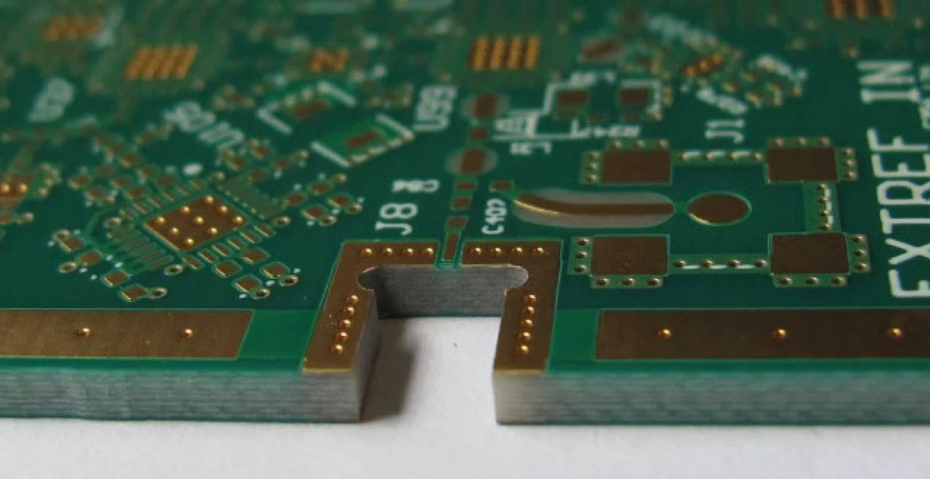
Via formation and plating in high-aspect-ratio structures
Via structures in thick copper PCBs present unique manufacturing challenges due to their extreme aspect ratios—the relationship between hole depth and diameter. While standard PCBs might feature aspect ratios of 6:1 or less, thick copper implementations commonly require ratios exceeding 10:1, particularly when connecting internal signal layers to heavy copper outer layers. These high-aspect-ratio structures demand specialized drilling and plating technologies to ensure reliable interconnections.
The drilling process for high-aspect-ratio vias requires precise control over drill bit concentricity, spindle speed, and withdrawal rates. Advanced entry and backup materials prevent copper burr formation and minimize drill bit wandering. For via diameters below 15 mil connecting to 6oz copper layers, controlled-depth drilling techniques may be employed, where initial pilot holes are created and subsequently enlarged to achieve optimal aspect ratios.
Plating these deep, narrow via structures presents perhaps the greatest manufacturing challenge in thick copper fabrication. Standard DC plating processes typically produce uneven copper distribution, with excessive buildup at via entrances and insufficient coverage at the center. Pulse-reverse plating technology has emerged as the preferred solution, alternating between forward plating cycles and brief reverse current pulses that selectively remove copper from high-density areas, producing more uniform via barrel plating even in extreme aspect ratios.
Controlled impedance manufacturing in heavy copper circuits
Maintaining controlled impedance specifications in thick copper circuits requires sophisticated manufacturing controls beyond those used in standard PCB production. The increased copper thickness creates complex electromagnetic field distributions that affect impedance characteristics, particularly for differential pairs and single-ended transmission lines. During design, field-solving software must account for the trapezoidal cross-section of etched traces, which becomes more pronounced as copper thickness increases.
Manufacturing processes must maintain exceptionally tight tolerances on dielectric thickness and consistency to achieve target impedance values. For a typical 50Ω controlled impedance microstrip line in 4oz copper, dielectric thickness variation must remain within ±5% to maintain impedance within a 10% tolerance band. This requires specialized lamination processes with precise pressure and temperature controls to prevent resin flow that could alter dielectric thickness under traces.
Test coupon designs for thick copper impedance verification require specific adaptations to account for the unique properties of heavy copper traces. Standard impedance testing methods using time-domain reflectometry (TDR) must be calibrated specifically for the trace geometries and material characteristics of thick copper implementations, with test fixtures designed to minimize transition effects that could mask actual impedance variations in the manufactured board.
Power electronics integration with thick copper technology
The rapid evolution of power semiconductor devices—particularly wide-bandgap technologies like silicon carbide (SiC) and gallium nitride (GaN)—has dramatically increased power density requirements for supporting PCB structures. Thick copper technology has emerged as an essential enabling technology for harnessing the full capabilities of these advanced semiconductor devices, providing the current handling capacity and thermal management necessary for optimal performance.
In high-frequency switch-mode power supplies operating in the 100kHz to 2MHz range, thick copper planes minimize power loop inductance while providing low-impedance current paths. A typical 5kW telecom power supply implemented with 6oz copper power planes can achieve power densities exceeding 50W/in³—nearly double what's possible with standard PCB technology. The reduced resistive losses translate directly to efficiency improvements of 1-2 percentage points, significant in applications where every fraction of a percent impacts operating costs and thermal management requirements.
Automotive applications: tesla model S/X inverter design implementation
Tesla's Model S and Model X vehicles showcase some of the most advanced implementations of thick copper PCB technology in electric vehicle power electronics. The main traction inverter—responsible for converting DC battery power to AC for the drive motors—utilizes thick copper PCBs to handle current levels exceeding 1000A during peak acceleration while maintaining compact dimensions essential for vehicle integration.
The design employs 10oz copper power planes in a compact sandwich structure connecting silicon carbide MOSFETs to DC link capacitors. This thick copper implementation achieves power loop inductance below 5nH—an essential parameter for minimizing switching losses and electromagnetic interference at high switching frequencies. The thermal management capabilities of the thick copper layers enable peak power handling exceeding 600kW in a package significantly smaller than conventional designs using standard PCB technology or busbars.
A particularly innovative aspect of Tesla's implementation involves selective use of copper thickness within the same board. Power distribution sections utilize full 10oz copper, while control and gate drive circuits employ standard 1oz-2oz copper on the same substrate. This mixed copper weight approach optimizes material usage, applying thick copper only where its benefits justify the additional cost. The design has proven remarkably reliable, with field data showing inverter failures below 10 parts per million—exceptional for such high-power electronics operating in demanding automotive environments.
Solar inverters and renewable energy control systems
Solar inverter technology has embraced thick copper PCBs to improve efficiency and power density while reducing system costs. Modern string inverters in the 30-100kW range typically employ 4oz-6oz copper for power conversion stages, enabling high efficiency that directly impacts the lifetime energy production of solar installations. The improved thermal characteristics of thick copper designs also contribute to extended lifespan in the challenging environmental conditions typical of solar deployments.
A notable implementation can be found in SMA's Sunny Tripower series, where thick copper PCB technology replaced conventional busbar designs in recent generations. The transition achieved a 30% reduction in converter volume while improving full-load efficiency from 97.8% to 98.4%. This efficiency improvement, though seemingly modest, translates to approximately 13MWh of additional energy production over a 25-year system lifespan for a typical 100kW installation—representing significant financial value.
Beyond performance improvements, thick copper PCB implementation has substantially reduced manufacturing complexity by integrating power distribution functions directly into the circuit board rather than requiring separate busbar assemblies. This integration has improved reliability by reducing the number of interconnection points while lowering assembly costs through automated manufacturing processes that weren't possible with previous discrete component approaches.
Military and aerospace grade thick copper implementations
Military and aerospace applications present some of the most demanding requirements for electronic systems, with extreme reliability expectations under harsh environmental conditions. Thick copper PCB technology has found extensive implementation in radar systems, electronic warfare equipment, and power distribution networks for aircraft and ground vehicles. These applications leverage not only the electrical and thermal advantages but also the enhanced mechanical strength that thick copper layers provide.
Airborne radar systems present a particularly compelling case study for thick copper implementation. Modern active electronically scanned array (AESA) radar systems incorporate hundreds of transmit/receive modules, each generating substantial heat during operation. Thick copper PCBs provide essential thermal management for these densely packed modules while simultaneously handling pulsed power distribution with minimal voltage drop. A typical implementation in F-35 Lightning II radar systems utilizes 6oz copper power distribution networks with aluminum core substrates, achieving thermal performance that would require significantly larger structures with conventional PCB technology.
Military ground vehicle power distribution systems represent another successful thick copper application area. In modern combat vehicles with high-power electronic systems, centralized power distribution units built on 10oz copper PCBs replace conventional wiring harnesses for secondary power distribution. These systems handle 28VDC distribution at currents exceeding 200A while providing intelligent load management and protection functions. The compact, integrated approach improves reliability in high-vibration environments while reducing weight and installation complexity compared to traditional wired solutions.
Medical device power management systems using heavy copper
Medical imaging and diagnostic equipment presents unique challenges for power management systems, requiring exceptional reliability while operating near sensitive detection equipment. Thick copper PCB technology has emerged as a key enabler for next-generation medical systems, providing low-noise power distribution with excellent thermal characteristics in compact form factors. These implementations must meet stringent safety and electromagnetic compatibility requirements while operating continuously for extended periods.
Advanced MRI systems utilize thick copper PCBs for gradient amplifier designs, handling current pulses exceeding 400A with minimal electromagnetic emissions that could interfere with sensitive imaging functions. A typical implementation employs 8oz copper planes with specialized EMI shielding structures integrated directly into the PCB design. The thick copper implementation achieves power density exceeding 40W/in³ while maintaining surface temperatures below 50°C without forced-air cooling—essential for the quiet operation required in clinical environments.
Portable medical devices present different challenges, with battery life and weight considerations paramount. Multi-modal patient monitors use 4oz copper designs to efficiently distribute power while minimizing voltage drops that would impact battery runtime. The mechanical strength provided by thick copper layers also enhances device durability, with field data showing a 45% reduction in failure rates due to drop damage compared to standard PCB implementations. This reliability improvement is particularly valuable in emergency medical applications where equipment durability directly impacts patient outcomes.
Cost-benefit analysis and design considerations
While thick copper PCB technology offers substantial performance advantages, these benefits must be weighed against increased manufacturing costs and design complexity. Understanding the complete cost implications—including material, fabrication, and lifetime operational factors—enables designers to make informed decisions about where thick copper technology provides genuine value. A comprehensive approach considers not just the immediate PCB cost differential but also system-level impacts on performance, reliability, and overall product lifecycle expenses.
Material cost comparison: 2oz vs. 10oz copper PCB production
The raw material cost differential between standard and thick copper PCBs represents the most immediate and visible cost factor. Copper pricing follows global commodity markets, with typical pricing around $8-10 per kilogram, translating to approximately $0.15-0.20 per square inch for each additional ounce of copper thickness on a standard 18" × 24" panel. For a typical 100 square inch PCB, increasing from 2oz to 10oz copper adds approximately $12-16 in direct copper material costs.
However, raw copper represents only a portion of the total cost differential. The specialized manufacturing processes required for thick copper fabrication typically double or triple the base manufacturing price compared to standard PCB production. A representative cost comparison shows that a 2oz copper design might cost $3-5 per square inch, while an equivalent 10oz implementation ranges from $9-15 per square inch—a premium of 200-300%. This cost differential decreases somewhat at higher production volumes but remains significant even for quantities in the thousands.
The true cost comparison must extend beyond the PCB itself to include system-level impacts on heat sinking, assembly complexity, and long-term reliability. These factors often offset much of the apparent price premium for thick copper implementations.
Design rule modifications for thick copper layouts
Designing for thick copper fabrication requires significant modifications to standard PCB design rules. These modifications ensure manufacturability while maximizing the performance benefits thick copper offers. The most fundamental adjustments involve trace width and spacing requirements, which increase substantially with copper thickness. For 6oz copper, minimum trace/space specifications typically start at 12mil/12mil—double or triple the minimums possible with standard 1oz copper.
Via design rules require particular attention in thick copper implementations. Aspect ratio limitations typically restrict via diameters to a minimum of 10mil for each 1oz of copper thickness they connect to, resulting in minimum via diameters of 60mil or larger when connecting to 6oz copper layers. These enlarged vias consume significant board area, requiring careful floorplanning to maintain reasonable circuit density. For high-density mixed-signal designs, via-in-pad techniques with filled and plated-over structures can recover some of the density lost to enlarged vias, though at additional manufacturing cost.
The increased copper thickness also impacts plated edge connectors, press-fit connections, and mechanical mounting features. Edge connector fingers in thick copper typically require additional beveling operations to ensure proper mating with standard connectors. Press-fit pins designed for standard PCB thicknesses may require upsized holes when used with thick copper boards. These mechanical considerations must be addressed early in the design process to avoid costly revisions after initial prototyping.
CAD tools supporting heavy copper design parameters
Standard PCB design tools require specific configuration to properly support thick copper implementations. Modern EDA platforms like Altium Designer, Cadence Allegro, and Mentor Pads include specialized settings for thick copper design rules, manufacturing outputs, and analysis capabilities. These tools enable designers to define copper-thickness-specific constraints that prevent design rule violations before they reach manufacturing.
Thermal simulation capabilities represent a particularly valuable feature for thick copper designs. Integrated thermal analysis tools in packages like Ansys SIwave and Siemens HyperLynx can model the impact of copper thickness on thermal spreading, helping designers optimize thermal performance without overspecifying copper weight. These simulation capabilities typically employ finite element analysis techniques that accurately represent the complex three-dimensional heat flow patterns in thick copper structures.
For stackup planning and impedance calculations, specialized tools like Polar Instruments' Si9000 provide accurate models of thick copper transmission line structures. These tools account for the trapezoidal cross-section of etched traces and the impact of copper thickness on electromagnetic field distributions. For designs mixing thick copper power distribution with high-speed signals, these accurate impedance predictions are essential for first-pass design success.
Total cost of ownership: thick copper vs. alternative solutions
Evaluating thick copper PCB technology against alternative approaches requires comprehensive total cost of ownership analysis that extends beyond immediate manufacturing expenses. Alternative solutions like busbars, wire bonding, or custom metal structures may appear less expensive initially but often incur higher system-level costs through increased assembly complexity, larger physical dimensions, or reduced reliability. A complete analysis must consider the entire product lifecycle from manufacturing through field operation.
In power supply applications, replacing discrete busbars with integrated thick copper PCB structures typically reduces assembly labor by 40-60% while improving first-pass test yields by 15-25%. Although the PCB itself costs more, the system-level savings often provide a net cost reduction of 10-20% when all manufacturing operations are considered. The improved reliability of integrated solutions further enhances the value proposition when warranty and service costs are included in the analysis.
For high-volume consumer products like smartphone chargers and laptop power adapters, the thermal management benefits of thick copper allow for size reductions that directly impact shipping costs. A typical 65W adapter implemented with 4oz copper can achieve a 30% volume reduction compared to a 2oz design with equivalent performance, reducing shipping costs by approximately $0.15-0.25 per unit. For products shipping in the millions, these logistics savings can completely offset the additional PCB manufacturing cost while providing a more compact product that enhances consumer appeal.
When properly analyzed across the entire product lifecycle, thick copper PCB technology often emerges as the most cost-effective solution for power electronics applications, despite higher initial PCB manufacturing costs. The combination of assembly simplification, improved reliability, and enhanced thermal performance typically delivers compelling financial benefits that justify the technology's adoption in increasingly diverse applications.